The most important real estate in the semiconductor industry is no longer the fab. It is the few square millimeters where finished dies are stitched together — and the geography of that work is being redrawn faster than any policy paper predicted.
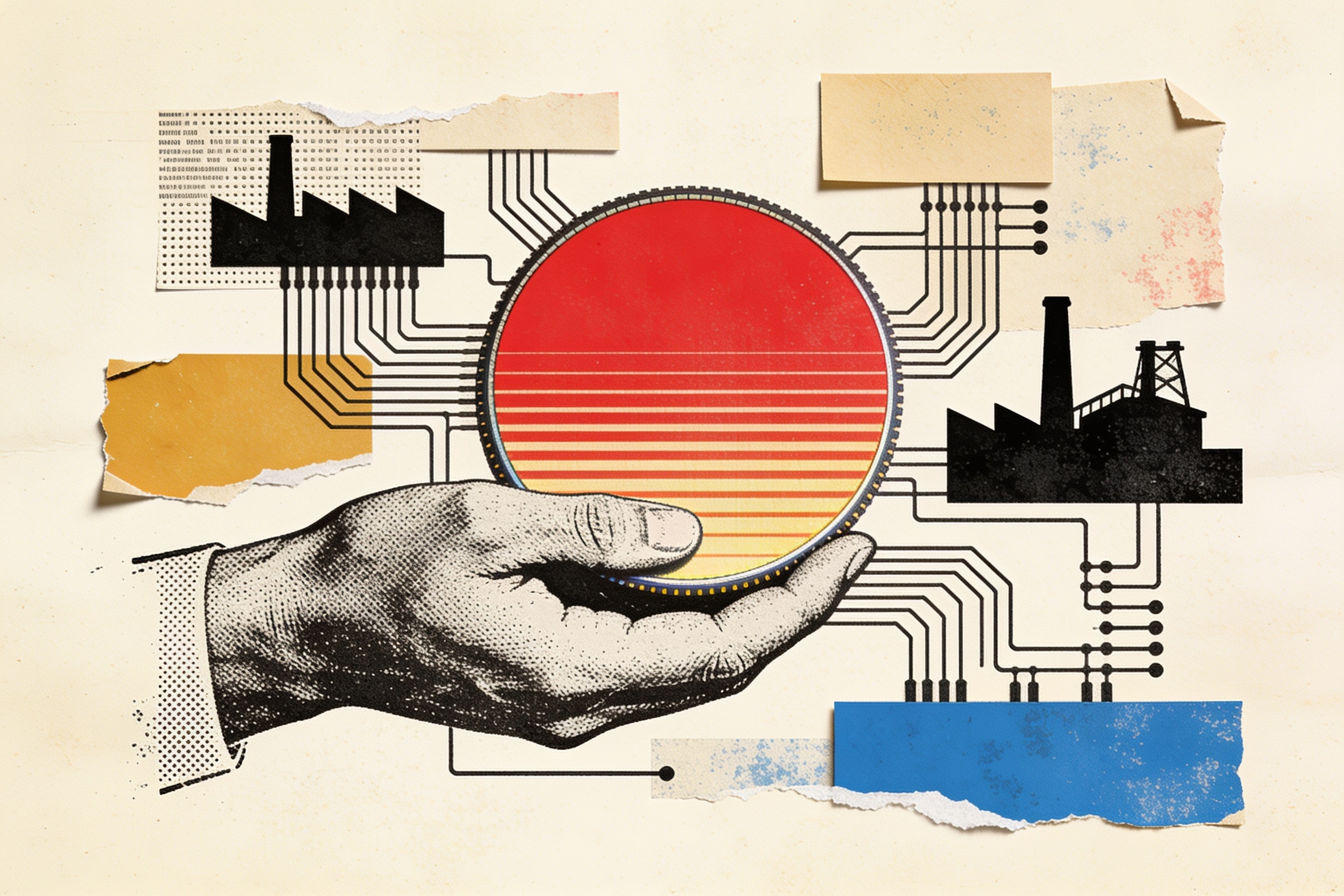
Advanced packaging was, for decades, the unglamorous end of the assembly line: take the chips, wire them up, seal the box. Then the physics of shrinking transistors got expensive enough that the industry found a cheaper source of performance — putting known-good dies closer together, stacking them vertically, and letting the package do work the wafer used to do.
The bottleneck moved
Every AI accelerator that matters today is constrained not by wafer starts but by advanced packaging capacity. The waiting list for high-bandwidth memory integration now stretches past fourteen months, and the fees command margins that would have been unthinkable for “assembly” work five years ago.
We spent a decade subsidizing fabs. The shortage showed up one building over.
Governments that fought the last war are discovering the new one has different trenches. The fabs got the headlines and the subsidies; packaging plants got neither, and the handful of firms that quietly built that capacity — in Taiwan, Malaysia, and a newly aggressive cluster in Arizona — are now naming their price.
Who saw it coming
The winners share a trait: they treated packaging as R&D rather than logistics. The firms that filed interconnect patents in 2021 are shipping products in 2026. The ones that outsourced “the easy part” are writing very large checks to their former contractors.
The second act of the silicon era will be decided by the boring buildings. The countries that understand this are not announcing it in press conferences — which is, itself, the tell.